Soubor:Wafer flats convention v2.svg

Původní soubor (soubor SVG, nominální rozměr: 150 × 150 pixelů, velikost souboru: 13 KB)
| Tento soubor pochází z Wikimedia Commons. Níže jsou zobrazeny informace, které obsahuje jeho tamější stránka s popisem souboru. |
Popis
| Popis |
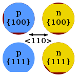
Wafer flats convention, based on Image:Wafer flats convention.PNG Conventional meaning of flats in semiconductor wafers. Red denotes material that has been removed. Wafer orientation is the orientation of the crystallographic plane in which the crystal grew. Wafer type indicated the type of doping.
|
| Datum | |
| Zdroj |
self-made, Tento vektorový obrázek byl vytvořen programem Inkscape . |
| Autor | Twisp |
| Další verze | Wafer flats convention.PNG |
Licence
| Já, autor tohoto díla, jej tímto uvolňuji jako volné dílo, a to celosvětově. V některých zemích to není podle zákona možné; v takovém případě: Poskytuji komukoli právo užívat toto dílo za libovolným účelem, a to bezpodmínečně s výjimkou podmínek vyžadovaných zákonem. |
Historie souboru
Kliknutím na datum a čas se zobrazí tehdejší verze souboru.
| Datum a čas | Náhled | Rozměry | Uživatel | Komentář | |
|---|---|---|---|---|---|
| současná | 24. 9. 2013, 23:40 | | 150 × 150 (13 KB) | Cepheiden | fixed position of secondary flat Silicon processing for the VLSI era - Vol. 1 - Process technology; S Wolf; RN Tauber - Lattice Press; 1986; ISBN 096167237; p. 23 |
| 23. 12. 2008, 02:37 |  | 150 × 150 (13 KB) | Inductiveload | Added arrow indication <110> direction and enlarged flats so they can be easily seen | |
| 29. 2. 2008, 23:17 |  | 150 × 150 (9 KB) | Twisp | ||
| 29. 2. 2008, 23:13 |  | 150 × 150 (9 KB) | Twisp | ||
| 29. 2. 2008, 23:06 |  | 150 × 150 (8 KB) | Twisp | ||
| 29. 2. 2008, 22:59 |  | 150 × 150 (8 KB) | Twisp | ||
| 29. 2. 2008, 20:09 |  | 150 × 150 (9 KB) | Twisp | {{Information |Description= Wafer flats convention, based on Image:Wafer flats convention.PNG Conventional meaning of ''flats'' in semiconductor wafers. Black denotes material that has been removed. Wafer orientation is |
Využití souboru
Tento soubor používá následující stránka:
Globální využití souboru
Tento soubor využívají následující wiki:
- Využití na ca.wikipedia.org
- Využití na de.wikipedia.org
- Využití na en.wikipedia.org
- Využití na es.wikipedia.org
- Využití na et.wikipedia.org
- Využití na eu.wikipedia.org
- Využití na fi.wikipedia.org
- Využití na it.wikipedia.org
- Využití na it.wikibooks.org
- Využití na ja.wikipedia.org
- Využití na ko.wikipedia.org
- Využití na nl.wikipedia.org
- Využití na pl.wikipedia.org
- Využití na ro.wikipedia.org
- Využití na sk.wikipedia.org
- Využití na uk.wikipedia.org
- Využití na www.wikidata.org